HyPerStripes – a successful final project review
HyPerStripes – a successful final project review The 16 partners of the EU project HyPerStripes (new assembly and interconnection technology for reliable bendable electronics) met at the end of March at OSYPKA AG in Rheinfelden, Germany, for the final project evaluation. The technological advances were summarized in presentations by each partner, and the final use case demonstrators were shown in live. In addition to the technological aspects, the sustainability of the new manufacturing processes was also assessed. The European reviewers and the representatives of the national funding organizations were impressed by the results achieved and the excellent cooperation within the consortium. Together, they developed and compared technologies for intelligent, flexible and large-scale electronic systems for five application demonstrators. Duration of the project: 01/04/2022 – 31/03/2025National funding: BMBF (16ME0469)Project Manager: Ulrike PasslackContact: passlack[at]ims-chips.de
Overview of the HyPerStripes Project
← Back to overview Overview of the HyPerStripes Project https://hyperstripes.ims-chips.de/wp-content/uploads/2024/12/Public-Presentation-HyPerStripes.mp4
Flexible and stretchable PCBs manufactured in Roll-to-Roll processes
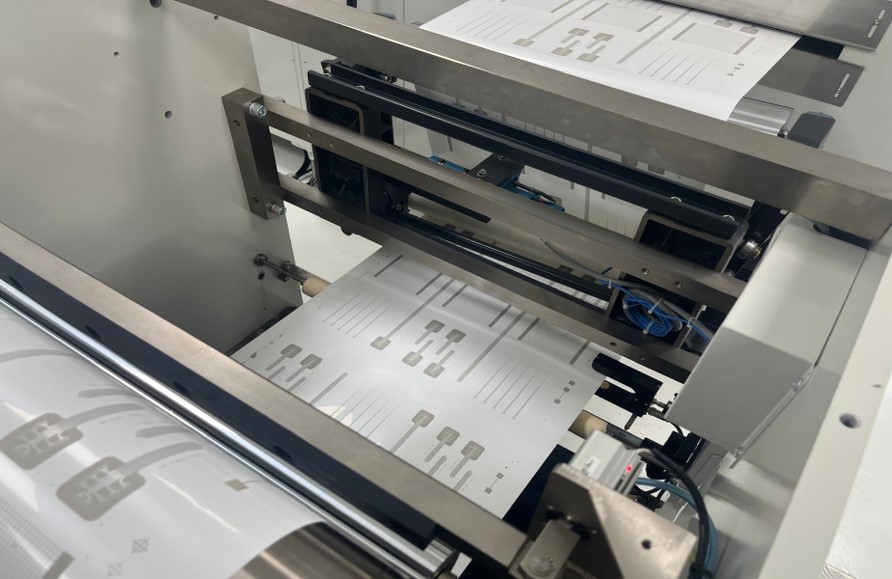
← Back to overview Flexible and stretchable PCBs manufactured in Roll-to-Roll processes R2R-Process Screen printing of silver and copper ink High resolution (towards transparent) ISO 8 cleanroom compatible. https://hyperstripes.ims-chips.de/wp-content/uploads/2024/11/Medien1.mp4https://hyperstripes.ims-chips.de/wp-content/uploads/2024/11/Medien2.mp4 Pixel-Soldering High strength interconnect Solder deposited Local heat introduced Solder flow and component allignement Roll-to-roll compatible https://hyperstripes.ims-chips.de/wp-content/uploads/2024/11/Medien3.mp4 TNO Netherlands Website
Roll-to-Roll manufacturing of dense copper traces on long flexible and stretchable foil stripes

← Back to overview Roll-to-roll manufacturing of dense copper traces on long flexible and stretchable foil stripes To produce cables of 1 meter or longer, we utilize our pilot line of roll-to-roll technology developed at Fraunhofer EMFT. The approach, combined with specialized R2R processes and machinery, enables the precise creation of metal patterns on flexible and stretchable substrates. A key component of this fabrication is the integration of a unique digital lithography stitching technique, which allows to produce high-quality, durable cables at extended lengths. The fabrication of the long cable consists of metal deposition on a flexible substrate, followed by lithography and etching (for Cu thickness up to 500 nm), or electroplating (for Cu thickness of 5-10µm). The semi-additive electroplating process enhances sustainability in metal patterning on flexible substrates by significantly reducing metal waste. In this process, metal thickness is selectively increased through electroplating, requiring only a thin seed layer, typically in the nanometre range, to be etched away. This contrasts with traditional methods, where thick metal layers—often several microns—are etched, generating substantial metal waste. By minimizing etching, the semi-additive process reduces both material consumption and chemical waste, making it a more environmentally friendly and resource-efficient alternative. © Fraunhofer EMFT © Fraunhofer EMFT/Bernd Müller Fraunhofer EMFT Germany Website
3D Geometry extraction and transformation
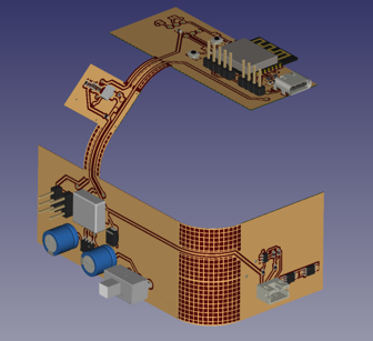
← Back to overview 3D Geometry extraction and transformation Project Focus 3D Geometry extraction and transformation (e.g. bending, spiraling) Simulations:→ data extraction: inductance, capacitance, resistance→ wave impedance for HF traces→ crosstalk / trace coupling Our fully Open-Source workflow enables designers to prepare simulations for predicting FPC performance and evaluating signal transmission. Model generation Geometries can be extracted from KiCad layout files, DXF, GDS, … Completely technology-agnostic process – can be used for etching, printing, … Geometries can be rendered and visualized Models can be transformed according to user-defined parameters Automatic mesh generation prepares geometries for simulations Thermal Simulations Elmer: Multiphysics simulations – Joule heat, heat transfer, warping, … HF Simulations, SI/PI Palace, OpenEMS, Qucs: HF Simulations (Reflectometry, Signal Integrity, Crosstalk, …) Our tool Our tool FTL („Fold the Line“) enables designers to create FPC models and, later, also prepare simulations automatically and retrieve results Technische Universität Dresden Germany Website
Chip-Film Patch Processing
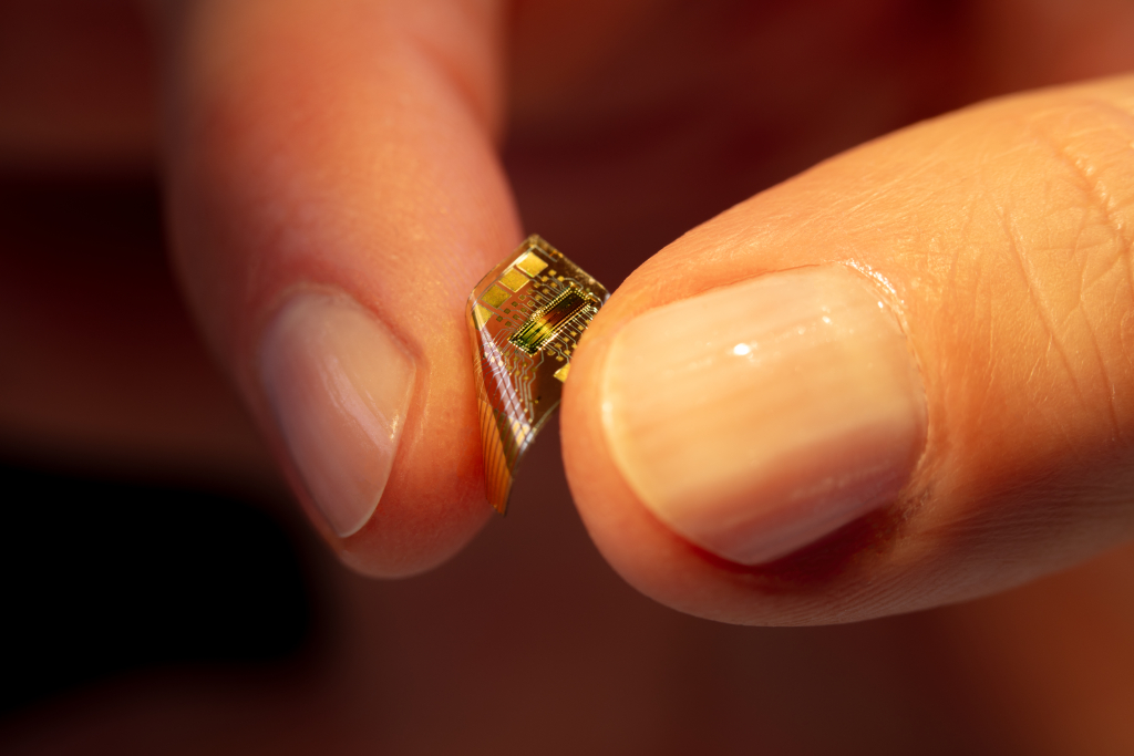
← Back to overview Chip-Film Patch Processing Unique Chip Embedding Technology Specifications of the Chip-Film Patch Fabrication Process Ultrathin Si Chips Applications Project: KoSiF Project: FFlexCom Ulrike Passlack Institut für Mikroelektronik Stuttgart Germany Website
Stretch.flex xS und xS-Ri: Sheet-2-Sheet (S2S) Processing
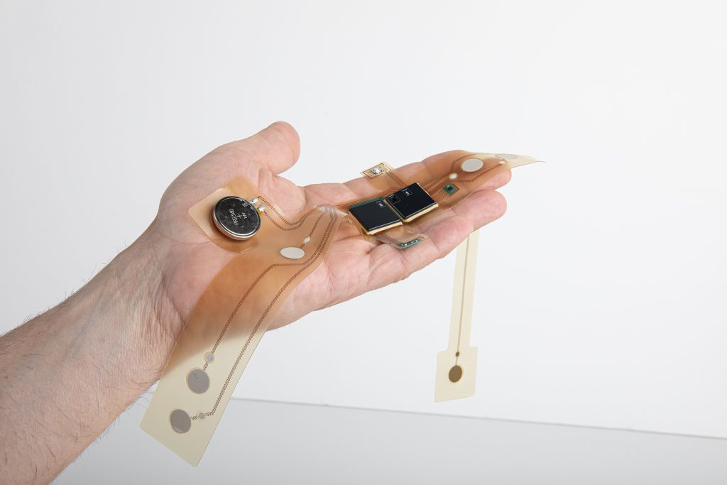
← Back to overview Stretch.flex xS und xS-Ri: Sheet-2-Sheet (S2S) Processing Material properties Extensive testing necessary Multiple rotation (n x 180°) without influence on stability and electrical properties Dynamic stretchability of 5 – 20 % Skin-friendly material Softening area: 155 – 185°C Multiple processing options (assembly in reflow, thermoforming/deep drawing, laminating…) Fields of application Medical Technology Sensor Technology Smart Textiles (Soft-) Robotics IoT (Internet of Things) Wearable Technology Würth Elektronik Germany Website
Hyperstripes meander patterns: Mechanical Simulation
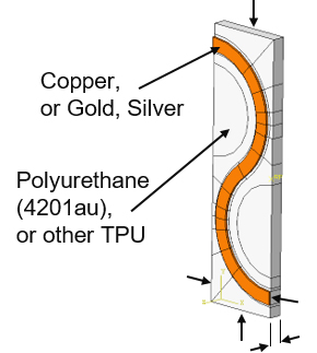
← Back to overview Hyperstripes meander patterns: Mechanical Simulation Introduction Patterns are used in the conductive tracks to create flexible electronics. The conductive materials, like Gold, Silver or Copper, typically are less strain-able than the substrate material they are placed on. The substrates (TPU’s) can take up to 100% strain easily, the conductors not (see figure #). Obviously, adding “length” to the conductive track would lead to an increase in resistance (and material use), and therefore undesirable in general. The pattern can therefore be designed as fit for purpose. To assess the strain-ability of the flexible conductors, Computer Design of Experiments (CDoE) were conducted. Finite Element Analysis models were made for HyPerStripes based on parametric models. Zhang et al., Procedia Eng. (2011) Wire thickness effects The plastic strain results in the conductor are plotted as a function of the applied strain to the HyPerStripe (ΔL/L0) For the typical horseshoe design (shown below) we observe in the tensile test different responses depending on the wire thickness. The thickest wire results here in the most stretchable design. Wire width effects Varied wire width: w The thinner wires compared to the w = 0.1mm case show interestingly more stretchability initially. The thickest wire develops plastic strain in the mid-section due to bending effects (1 & 2). Depending on the amount of stretch, the thinner wires develop for the large strain case, (2), mainly plastic equiv. strain around the tops. Design optimization As a basis for the parametric models, tow possible design are evaluated, a horse-shoe like design and a block shaped design. The relatively straight-forward designs have up to 6 design parameters which were varied, keeping the polyurethane substrate material (4201AU by Covestro) and the conductor base material (Copper) constant. These materials can be replaced by others in the CDoE. From the mechanical point of view, the plastic strain in the conductive material was used as the critical parameter for assessing the “performance” of each design. The conductivity of the track was assumed to be unchanged up to the failure strain of the conductors. Design tool For designing, the engineer would probably ask: “what is the design we need to fulfil the requirements”. To answer this question, the results of the CDoE are made available to Design Space Exploration (DSE) software. The results is that the engineer can define the requirements and gets the design back as a solution. M. Assen, E. Lamers Reden BV Netherlands Website
Xecs Matchmaking Event
Xecs Matchmaking Event The Xecs Matchmaking Event will take place on October 15th in Hamburg, Germany. Our HyPerStripes partners Corne Rentrop (TNO) and Christof Landesberger (Fraunhofer EMFT) will showcase HyPerStripes in a poster presentation and promote our follow-up project. Xecs Matchmaking Event – Xecs Call 4 : Aeneas (aeneas-office.org)
Techblick 2024
Techblick 2024 The conference will take place from October 23th to the 24th in Berlin, Germany. Our HyPerStripes partner, Stefan Bendig from Würth Electronic, will give a presentation on „State of the art of the industrial stretchable PCB and its potential for future development” https://www.techblick.com/electronicsreshaped
